

Germanium Substrates in Optoelectronics and High-Frequency Communications: Technical Barriers and Application Prospects

Germanium (Ge), as a Group IV semiconductor, has attracted sustained attention in optoelectronics and high-frequency communications due to its compatibility with silicon processing, high carrier mobility, and strong near-infrared absorption. However, the transition from laboratory to industrialization faces multiple technical barriers in LED and laser manufacturing, while Ge-based devices are demonstrating breakthrough potential in high-frequency communications.
I. Core Technical Barriers in LED and Laser Manufacturing
1. Lattice Mismatch and Threading Dislocation Density Control
Significant lattice mismatch exists between Ge substrates and III-V compound semiconductors (such as GaAs and InP). The lattice mismatch between GaAs and Ge is approximately 0.07%, yet threading dislocation densities during epitaxy can reach 10⁷–10⁸ cm⁻². Research shows that through buffer layer optimization, the average dislocation density in a 1.5 µm Ge layer can be reduced from ~10⁸ cm⁻² by over three orders of magnitude, approaching a lower limit of ~10⁴ cm⁻².
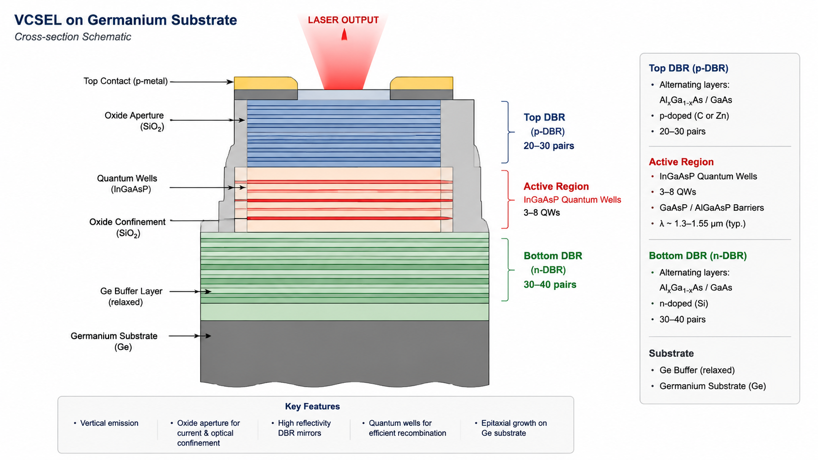
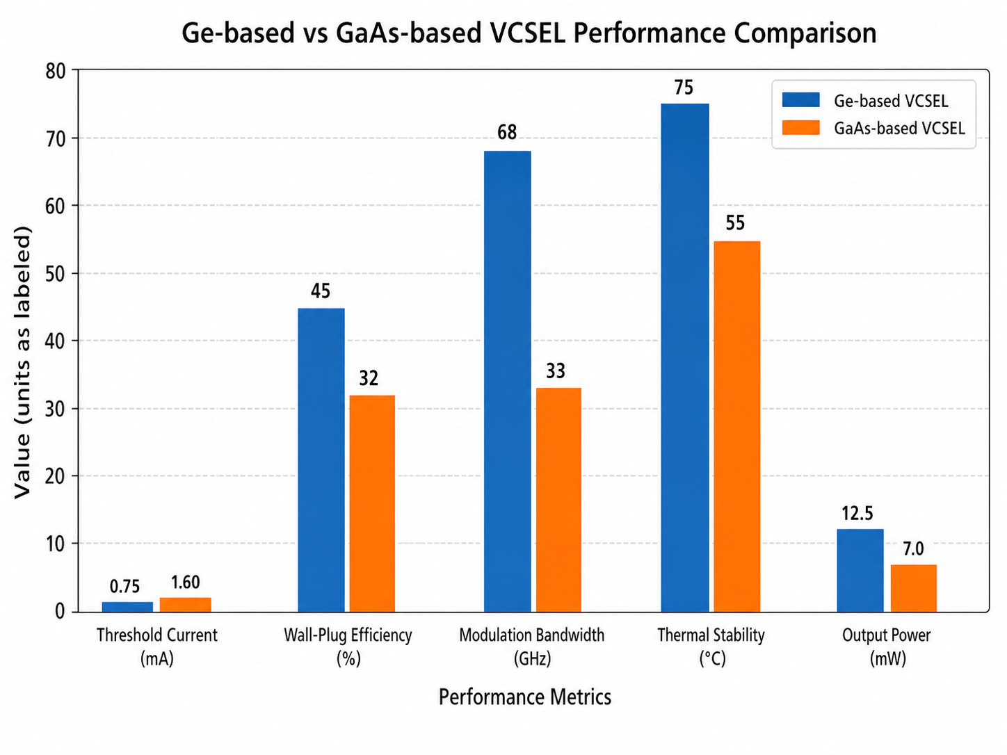
An April 2026 study systematically developed an independent Ge-based VCSEL technology route and comprehensively benchmarked it against GaAs-based devices. The half-VCSEL structure on engineered Ge substrates successfully suppressed anti-phase domains, achieving a surface roughness of 0.84 nm. However, Ge-based VCSELs still face lower yield and larger performance variation. Accumulated stress and defect control in buried multiple quantum wells are essential for improving yield, uniformity, and reliability.
2. Anti-Phase Domain Problem
When epitaxially growing III-V polar semiconductors (such as GaAs) on Ge substrates, anti-phase domains tend to appear at the interface—regions where Ga and As atoms interchange positions in the lattice. These anti-phase domain boundaries form electrically active defects that severely impact device performance. High-temperature pretreatment of the Ge substrate surface in an As or P atmosphere can effectively prevent anti-phase domain formation.
3. Thermal Expansion Mismatch and Wafer Bow
Thermal expansion coefficient differences between Ge and III-V materials generate thermal stress during post-epitaxy cooling, causing wafer bow. Interestingly, this is where Ge substrates offer a distinct advantage—Ge-based VCSELs demonstrate 72% reduction in wafer bow/warp and 40% reduction in surface roughness compared to GaAs-based counterparts. The best Ge-based devices exhibited 19% higher differential efficiency.
4. Indirect Bandgap Nature of Germanium
Germanium is an indirect bandgap semiconductor with inherently lower luminescence efficiency than direct bandgap III-V materials. Applying tensile strain can transform Ge into a direct bandgap material. Through strain engineering, research teams have introduced 3% uniaxial tensile strain in Ge microbridge LEDs, achieving peak electroluminescence at 1986 nm with an electro-optical conversion efficiency of 1.94%.
5. Material Brittleness and Processing Difficulty
Germanium is relatively brittle and prone to fracture during large-diameter wafer processing-, requiring more precise cutting, grinding, and polishing processes, increasing manufacturing costs and complexity.
II. Frontier Application Progress
Ge-Based VCSELs Toward Larger Diameters: Ge substrates offer a viable path to scale VCSELs to 8-inch and 12-inch wafers. In July 2025, researchers successfully grew 940 nm VCSEL structures on 150 mm (6-inch) Ge substrates with thicknesses as thin as 225 µm.
Mid-Infrared LED Breakthrough: A March 2026 study published in Advanced Optical Materials achieved 3.8 µm mid-infrared LED emission using PbSe/GaAs hybrid heterojunctions, with pulsed output power reaching 400 µW. The devices functioned despite threading dislocation densities on the order of 10⁹ cm⁻².
Quantum Cascade Laser Hybrid Integration: An April 2026 study demonstrated hybrid integration of quantum cascade lasers with germanium-on-silicon waveguides, achieving end-fire coupling efficiencies of up to 50% through flip-chip bonding.
III. Applicability in High-Frequency Communication Devices
Core Advantages of Germanium in High-Frequency Applications
Germanium possesses high hole and electron mobility and strong optical absorption coefficients in communication bands-, giving Ge-based materials natural advantages in high-speed electronic and optoelectronic devices.
2026 Milestone Breakthrough: Silicon-Graphene-Germanium Barristor
On June 6, 2026, a team led by Sun Dongming and Liu Chi from the Institute of Metal Research, Chinese Academy of Sciences, published a major breakthrough in high-frequency transistors in Nature Communications. This represents the world’s first barristor to successfully achieve RF testing.
Technical Approach: The team first epitaxially grew wafer-scale single-crystal monolayer graphene on a Ge substrate via chemical vapor deposition, then precisely stacked single-crystal silicon film on top, constructing a high-quality silicon-graphene-germanium vertical heterostructure. Utilizing asymmetric Schottky barriers at the graphene-silicon and graphene-germanium interfaces, combined with graphene’s quantum capacitance effect for work function modulation, the current variation at the germanium end far exceeds that at the silicon end.
Performance Metrics:
- Common-emitter current gain: 1.8×10⁷, setting a new world record among reported transistors
- Intrinsic cutoff frequency: 132 GHz, surpassing the highest level of all previous vertical two-dimensional base transistors
- Theoretical operating frequency: Through optimizing material doping concentration, reducing contact resistance, and minimizing parasitic effects, the device is projected to exceed 1 THz, entering terahertz application bands
- Significance for 6G Communications: With large-scale 5G deployment and accelerated 6G research, IoT, intelligent sensing, and high-speed communications require transistor operating frequencies exceeding 1 THz. This research lays the foundation for barristor applications in RF and terahertz communications, opening new technological pathways for future IoT, 6G sensing systems, and ultra-high-speed signal processing.
IV. Market Trends and Strategic Value
Price Trends: As of late June 2026, Changjiang Nonferrous Metals Network quoted germanium at RMB 23,150–23,550/kg, averaging RMB 23,350/kg. Domestic 5N high-purity germanium ingots have stabilized at RMB 25,000/kg, an 83% increase from year-end 2025. Fiber-grade germanium tetrachloride has risen nearly 300% year-to-date.
Substrate Market: Global single-crystal germanium wafer capacity reached 1.45 million pieces in 2025, with actual production of approximately 1.2 million pieces and average market price of approximately **$650 per piece**, with gross margins primarily in the 25%–38% range. Indium phosphide substrate prices: 3-inch at RMB 2,300–3,500/piece, 4-inch at RMB 5,500–8,000/piece, 6-inch at RMB 18,000–20,000/piece. 2-inch optical communication-grade products have risen from $800/piece in early 2025 to $2,300–2,500/piece.
Supply Landscape: Germanium’s primary supply comes from zinc smelting byproduct recovery systems, with supply elasticity constrained by both main metal smelting节奏 and recovery purification capacity. China implements export licensing/dual-use item controls on germanium and certain germanium products. Germanium’s irreplaceability in infrared optics (thermal imaging substrate lenses), fiber optics (GeCl₄ doping), and space/high-end electronics (satellite power/detectors) makes it a quintessential “strategic bargaining chip”
