Rhenium in the Electronics Industry: Applications, Performance, and Strategic Supply Dynamics
Abstract:
Rhenium, one of the rarest elements in the Earth‘s crust with an annual global production of merely 50–60 tonnes, has traditionally been associated with aerospace superalloys. However, its unique combination of properties—a melting point of 3186°C, exceptional corrosion resistance, and high electrical conductivity—positions it as an increasingly critical material in the electronics industry. This white paper provides a comprehensive analysis of rhenium’s applications in electronics manufacturing, encompassing sputtering targets, high-temperature conductive thin films, vacuum electronic devices, precision thermocouples, catalysts for electronic-grade chemicals, and emerging two-dimensional semiconductors. Market data and research breakthroughs up to May 2026 are systematically integrated.
1. Introduction
Rhenium (Re), element 75, is the last stable element discovered in nature. With a crustal abundance of approximately 1 part per billion, it is among the scarcest metals on Earth. Global explored reserves total approximately 2,500–2,600 tonnes, and annual primary production is confined to 50–60 tonnes, recovered exclusively as a by-product of copper and molybdenum smelting.
While approximately 80% of global rhenium consumption is directed toward aerospace superalloys—primarily nickel-based single-crystal turbine blades—the electronics industry represents a growing and technologically significant demand segment. This white paper examines rhenium‘s established and emerging roles in electronics manufacturing, drawing on peer-reviewed research published through May 2026 and the latest market intelligence.
2. Physical Properties Relevant to Electronics Applications
Rhenium’s value in electronics derives from:
| Property | Value | Source |
| Melting Point | 3186°C | [19†L8-L9] |
| Boiling Point | 5596°C | [19†L8-L9] |
| Electrical Resistivity (20°C) | 19.3 μΩ·cm | [25†L9-L10] |
| Crystal Structure | Hexagonal close-packed (HCP) | Standard reference |
| Crustal Abundance | ~1 ppb | [18†L4-L5] |
3. Core Applications in the Electronics Industry
3.1 Sputtering Targets for Semiconductor and Display Manufacturing
Rhenium sputtering targets represent the most commercially established electronics application. Through physical vapor deposition (PVD), high-purity rhenium targets deposit functional thin films onto semiconductor wafers and display panel substrates.
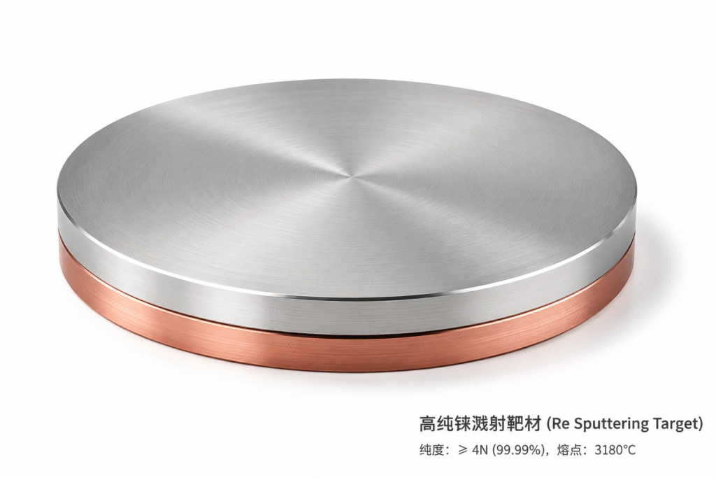
Molybdenum-rhenium (Mo-Re) alloy targets combine molybdenum‘s high melting point with rhenium’s superior ductility and corrosion resistance. The addition of rhenium significantly mitigates the brittleness of pure molybdenum targets, reducing cracking during fabrication and use while improving sputtering efficiency and film adhesion. These targets serve as electrode materials in OLED production, ensuring high brightness and low power consumption, and enhance photovoltaic conversion efficiency in solar cell manufacturing.
Rhenium also serves as an evaporation material in the form of wire, pellets, or targets, deposited via electron-beam or thermal evaporation to create high-temperature alloy coatings and optical reflective films-.
Major global producers include American Elements, Kurt J. Lesker, Stanford Advanced Materials, ALB Materials Inc, MSE Supplies, and several Chinese rare metal manufacturers.
3.2 High-Temperature Conductive Thin Films
A landmark study published in Scripta Materialia (April 2025) by Xi‘an University of Technology and Jinduicheng Molybdenum Co. investigated rhenium’s effect on the high-temperature stability and conductivity of molybdenum-based thin films.
Key findings from Mo-Ta-Re versus Mo-Ta-Ni comparative experiments:
- Conductivity enhancement: Mo-Ta-Re films exhibited 47% lower resistivity (95 vs. 181 Ohm·nm). After 700°C annealing, the Re-containing film‘s resistivity further decreased to 82 Ohm·nm.
- Thermal stability: The Re-containing film maintained structural integrity at 700°C, while the Ni-containing film suffered 76% resistivity increase due to selective tantalum oxidation and exhibited delamination.
- Atomic mechanism: Density functional theory calculations revealed strong d-orbital hybridization between Re-Ta atoms forming stable metallic bonds, contrasted with repulsive Ni-Ta interactions.
The research team noted that “the high conductivity and resistance to high-temperature degradation of rhenium alloy films can significantly enhance the reliability and lifespan of critical components such as TFT-LCD gate electrodes and PCB circuitry”.
3.3 Vacuum Electronic Devices
Rhenium’s application in vacuum electronic devices—electron tubes, electron guns, cathode-ray tubes—spans decades. Its ultra-high melting point and low vapor pressure enable stable thermionic electron emission under extreme thermal conditions, substantially extending device service life. Rhenium components are integral to electron sources in mass spectrometers and electron microscopes, appear as coatings on rotating anodes in X-ray tubes, and serve critical functions in electronic emitters and electrical contacts aboard spacecraft and space physics instrumentation.
3.4 Precision Thermocouples and High-Temperature Heating Elements
Tungsten-rhenium (W-Re) thermocouples, capable of measuring temperatures up to 2800°C, are indispensable temperature sensors in nuclear power, space launch, and high-temperature semiconductor process monitoring.
In semiconductor manufacturing, rhenium-based heating elements are deployed in MOCVD equipment to provide precise temperature control during epitaxial growth. Domestically produced tungsten-rhenium heating elements for MOCVD were exhibited by Chinese manufacturers at SEMICON China 2025-. Rhenium components also feature in ion implantation equipment and rapid thermal processing systems.
3.5 Catalysts for Electronic-Grade Chemical Synthesis
Rhenium-based catalysts play a growing role in the synthesis of high-purity chemicals for electronics manufacturing. In December 2025, Zhejiang Normal University and Zhejiang Juhua Technology Center filed a patent (CN121402078A) for a nano-scale highly dispersed rhenium-based catalyst designed for perfluorobutyl ethylene production.
The catalyst operates with only 0.1–1 wt% rhenium loading at particle sizes of 0.1–10 nm, achieving efficient activation under mild conditions with easy separability and recyclability—suitable for continuous industrial production. Perfluorobutyl ethylene serves as a critical intermediate in advanced fluorinated electronic materials.
Additionally, a 2026 patent (CN121853018A) by GRINM Group disclosed a PEM water electrolysis catalytic electrode incorporating rhenium doping into a manganese-based non-precious metal catalytic system, eliminating dependence on iridium.
3.6 Emerging Two-Dimensional Rhenium-Based Semiconductors
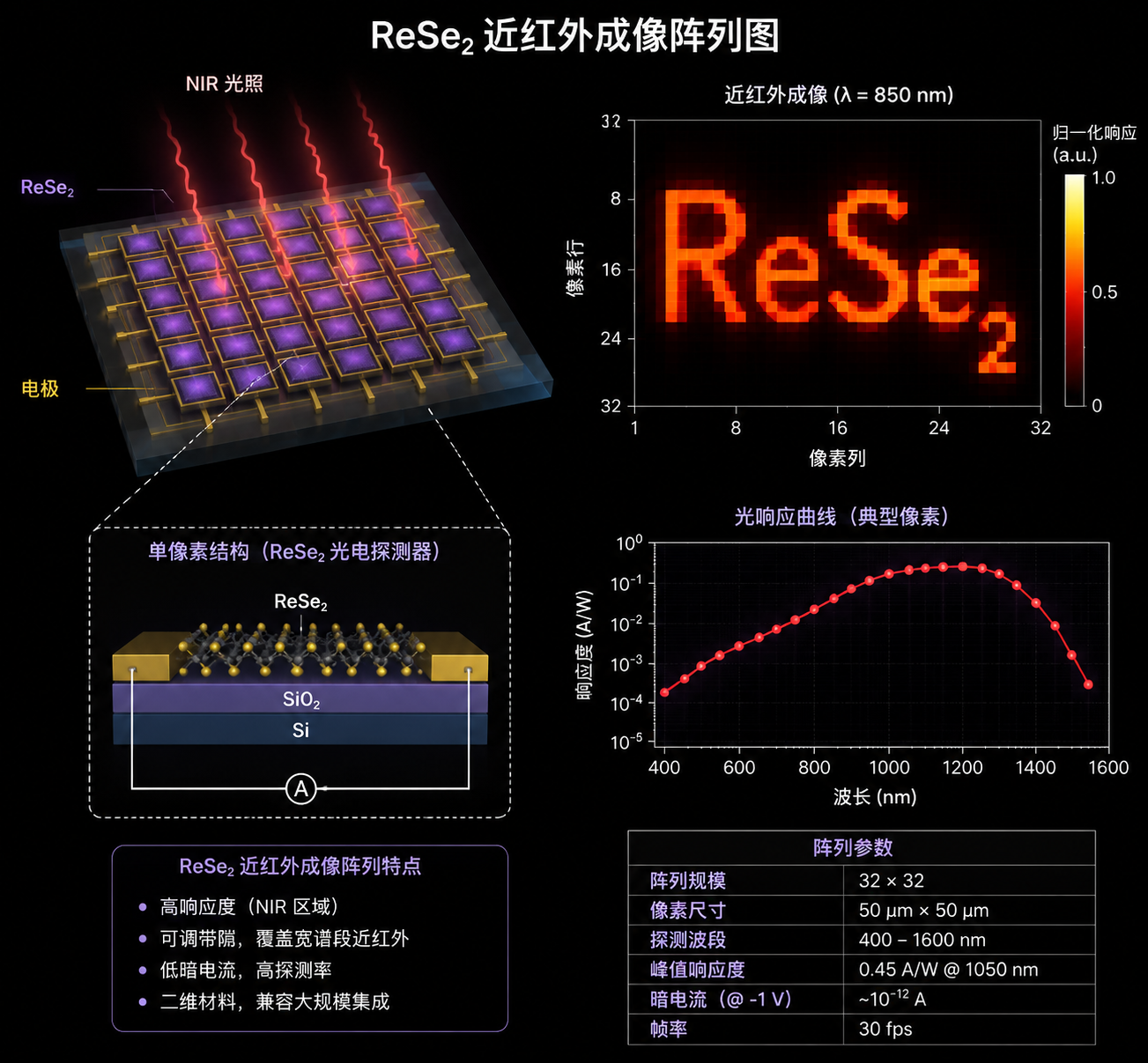
Rhenium diselenide (ReSe₂) has emerged as a promising two-dimensional semiconductor material for near-infrared optoelectronics. ReSe₂ exhibits p-type transport behavior—rare among transition metal dichalcogenides—and a narrow bandgap of 0.9–1.0 eV, endowing it with exceptional near-infrared detection capability.
In August 2025, a team at Fudan University reported a breakthrough in Advanced Materials Technologies: a BiOCl-assisted low-temperature chemical vapor deposition process enabling centimeter-scale, monolayer-uniform ReSe₂ film growth on sapphire substrates. A 4×4 near-infrared imaging array was successfully demonstrated.
This low-temperature synthesis route resolves the critical BEOL thermal compatibility challenge that previously constrained integration of rhenium-based 2D materials with silicon CMOS platforms.
4. Market Dynamics and Supply-Demand Outlook
4.1 Supply Structure
Global primary rhenium production is structurally inelastic, derived entirely as a by-product of copper-molybdenum smelting. Annual output is confined to 50–60 tonnes. Production is highly concentrated: Chile accounts for over 50% of global output, with the United States and Poland collectively contributing most of the remainder-. China‘s rhenium reserves are estimated at approximately 200 tonnes (7.7% of global total), characterized by low-grade, complex paragenetic deposits.
China’s domestic rhenium mine output reached 20 tonnes in 2025, representing 24.69% of the global total—a 277% year-on-year increase marking a substantive shift from import dependence toward domestic production capability.
4.2 Demand Dynamics
China‘s rhenium consumption structure comprised approximately 78% superalloys, 12% catalysts, and 10% electronics and other applications in 2023. The electronics segment, while modest in absolute volume, is experiencing exponential demand growth driven by semiconductor and display manufacturing expansion.
Projections indicate that China’s rhenium demand will reach 53.3 tonnes by 2043, while domestic primary production capacity is estimated at only 22.3 tonnes, creating a structural deficit of approximately 58%.
4.3 Price Trends and Policy Developments
Rhenium prices have undergone significant revaluation. As of February 2026, metallic rhenium reached RMB 45,000/kg, a cumulative increase exceeding 150% from approximately RMB 18,000/kg in early 2025. In Q1 2026, rhenium prices recorded a 113% year-on-year and 38% quarter-on-quarter increase.
The U.S. Defense Logistics Agency executed two rounds of rhenium procurement totaling approximately 90 tonnes during 2025-2026, equivalent to roughly 2.5 years of global primary production. China is simultaneously advancing spent turbine blade rhenium recycling infrastructure and evaluating the inclusion of rhenium in its national strategic stockpile system-.
The global high-purity rhenium metal market was valued at approximately USD 179 million in 2025, projected to reach USD 221 million by 2032 (CAGR approximately 3.0%). Product grades span 3N, 4N, and 5N purity, serving high-temperature components, catalysts, and other applications respectively.
5. Conclusion and Outlook
Rhenium‘s role in the electronics industry is evolving from a niche auxiliary material into a strategically significant enabling element. The application landscape encompasses:
| Application | Material Form | Maturity | 2025-2026 Notable Development |
| Sputtering Targets | Pure Re / Mo-Re alloy | Commercial production | Expanding OLED/semiconductor demand |
| High-Temp Thin Films | Mo-Ta-Re alloy films | Laboratory breakthrough | 47% lower resistivity; 700°C structural integrity |
| Vacuum Electronic Devices | Metallic Re / Re coatings | Mature | Continued use in X-ray tubes, mass spectrometers |
| Thermocouples & Heating Elements | W-Re alloys | Commercial production | Domestic MOCVD heater debut at SEMICON 2025 |
| Electronic Chemicals Catalysis | Re-based nanocatalysts | Pilot stage | Perfluorobutyl ethylene patent granted |
| 2D Semiconductors | ReSe₂ / ReS₂ thin films | Fundamental research | cm-scale monolayer film + 4×4 NIR imaging array |
Looking forward, five trends merit attention:
- Sputtering target consumption growth driven by advanced semiconductor nodes and OLED capacity expansion
- Commercialization of Re-containing high-temperature conductive thin films for 5G/6G, automotive electronics, and aerospace electronics
- Continued advancement of ReSe₂/ReS₂-based infrared sensors and anisotropic electronic devices toward practical deployment
- Strengthened closed-loop recycling of rhenium from end-of-life aerospace components, indirectly securing electronics industry supply
- Persistent structural supply deficit sustaining upward price pressure and reinforcing rhenium‘s status as a strategic critical mineral
This white paper reflects data current as of May 2026. For further technical inquiries, please contact the company research department.
