Title: Hafnium in Electronic Devices: Performance, Applications, and Technological Frontiers
Abstract:
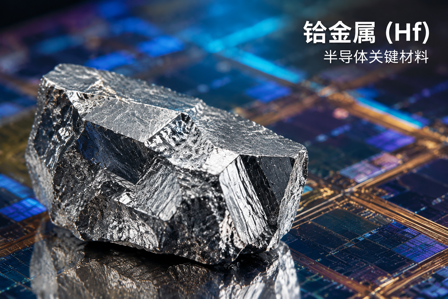
Hafnium (Hf), a transition metal once confined to niche nuclear applications, has become a cornerstone material in advanced semiconductor manufacturing. Its oxide form (HfO₂) serves as the industry-standard high-k gate dielectric in logic nodes from 45nm down to 3nm and beyond, while doped hafnium-based films are enabling next-generation ferroelectric non-volatile memories and in-memory computing architectures. This white paper provides a comprehensive analysis of hafnium‘s applications in electronic devices, integrating the latest market data and research breakthroughs up to April 2026.
1. Introduction
The semiconductor industry’s relentless drive toward miniaturization has placed extraordinary demands on materials science. When silicon dioxide (SiO₂) gate dielectrics reached their physical limits at the 45nm technology node, hafnium-based high-k materials emerged as the enabling solution. Since Intel‘s landmark introduction of HfO₂-based gate dielectrics in 2007, hafnium has become irreplaceable in advanced CMOS manufacturing.
In recent years, the discovery of ferroelectricity in doped HfO₂ has opened an entirely new application space for hafnium-based materials in non-volatile memory and neuromorphic computing. This white paper examines the current state and future trajectory of hafnium’s role in electronic devices, drawing on the latest peer-reviewed research and industry data.
2. Material Properties and Key Performance Metrics
Hafnium serves the electronics industry primarily through its oxide (HfO₂) and related compounds. The critical performance parameters of HfO₂ are:
| Property | Value | Source |
| Dielectric Constant (κ) | 20-25 | [12†L10-L11] |
| Bandgap | ~5.8 eV | [10†L35-L37] |
| Melting Point | ~2780-2800°C | [21†L10] |
| Refractive Index (at 500nm) | ~2.0 | [21†L8] |
| Optical Transmission Range | 220-12000 nm | [21†L8] |
| Breakdown Field | ~22.3 MV/cm (ultra-thin films) | [8†L16-L18] |
HfO₂ exists in three crystal structures—monoclinic, tetragonal, and cubic—with the orthorhombic phase (Pca2₁) responsible for ferroelectric behavior when stabilized through doping with Zr, Si, or Al.
3. Core Application I: High-k Gate Dielectrics
3.1 Technology Background
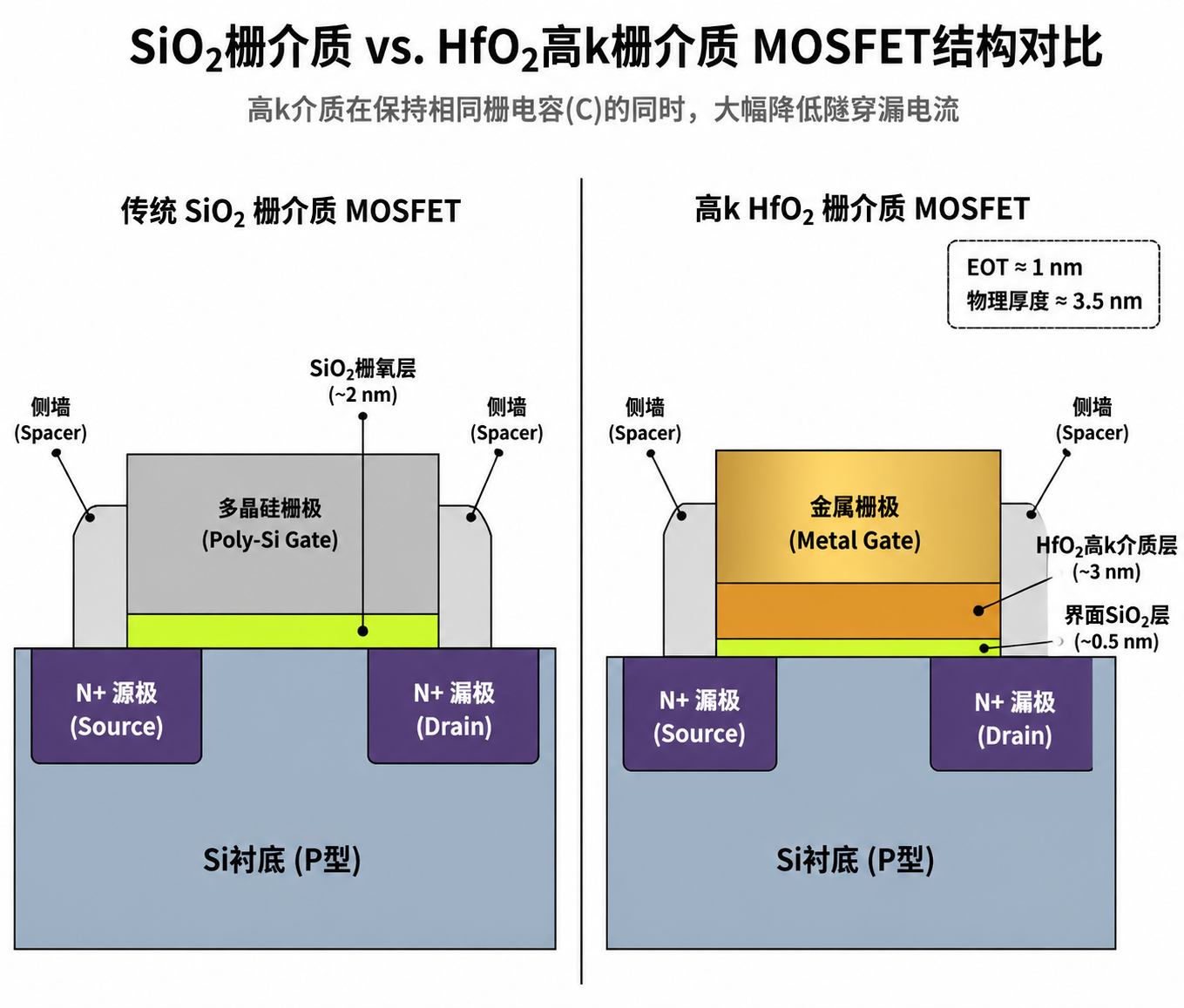
As CMOS technology scaled below 45nm, SiO₂ gate dielectrics thinned to less than 2nm, resulting in exponential increases in gate leakage current due to quantum mechanical tunneling. Hafnium-based high-k materials solve this problem by providing equivalent capacitive coupling at greater physical thickness.
Hafnium silicate (HfSiO₄) has been successfully deployed in CMOS technology at 45nm and below. At the 28nm node, HKMG technology using HfO₂-based materials achieved a greater than 100-fold reduction in gate leakage compared to traditional SiO₂/polysilicon stacks. Major foundries including TSMC have publicly confirmed the use of hafnium-based dielectrics in their 5nm and 3nm process nodes.
3.2 2025-2026 Breakthrough: Sub-5-Å EOT HfO₂ Dielectrics
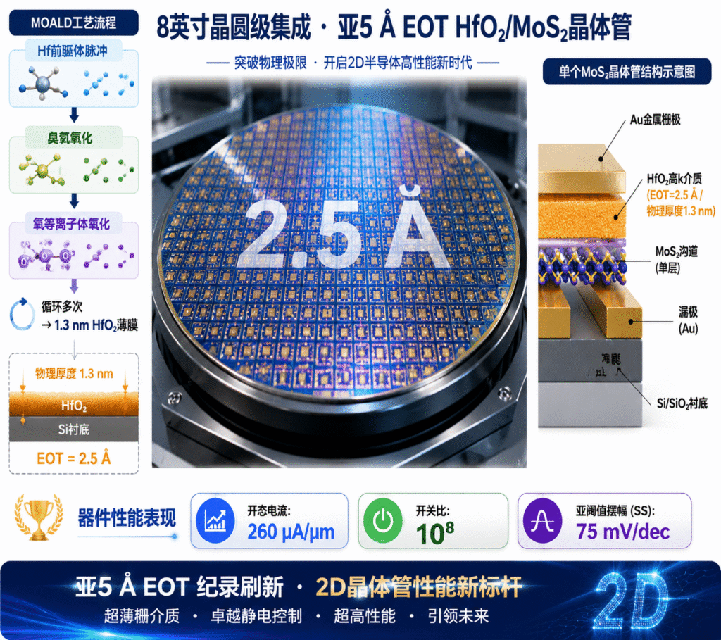
In April 2026, a collaborative international team led by the Songshan Lake Materials Laboratory and the Institute of Physics, Chinese Academy of Sciences, published a landmark study in Nature Communications demonstrating wafer-scale HfO₂ dielectric films with sub-5-Å equivalent oxide thickness (EOT) for 2D MoS₂ transistors.
The team developed an industry-compatible multiple oxidation atomic layer deposition (MOALD) process at 200°C, achieving:
- Physical thickness: 1.3 nm
- EOT: 2.5 Å (among the lowest ever reported)
- Leakage current: ~10⁻⁶ A/cm²
- Breakdown field: ~22.3 MV/cm
- Dielectric constant: 19.8
The 8-inch wafer-scale integrated MoS₂ FETs exhibited: on-state current density of 260 µA/µm at Vds=0.5V, on/off ratio of 10⁸, average subthreshold swing of 75 mV/dec, and successfully demonstrated inverters, AND/NAND/NOR gates, and 5-stage ring oscillators. The inverter achieved a gain of 205 at 1V. This work provides a practical pathway toward the 2037 targets outlined in the International Roadmap for Devices and Systems (IRDS).
3.3 Leakage Current Suppression: ALHM Method (2025)
A study published in Materials Science in Semiconductor Processing (July 2025) proposed an atomic layer hydrogen manipulation (ALHM) method—in-situ, layer-by-layer H₂ plasma treatment during ALD deposition of HfO₂. The technique reduced gate leakage current density by six orders of magnitude while improving film density and device reliability.
3.4 DRAM Capacitor Dielectrics: VHF PE-ALD HZO (2025)
Research published in Journal of Materials Chemistry C (February 2025) demonstrated 4.5nm HZO films fabricated by 100MHz VHF PE-ALD for DRAM capacitor applications, achieving superior crystalline quality with minimized oxygen vacancies-.
3.5 HZO Superlattice for GAAFETs
Composition-dependent Hf₁₋ₓZrₓO₂ superlattice structures with NH₃ plasma-optimized interfaces have been developed for Si nanosheet gate-all-around FETs (NSGAAFETs). Ferroelectric HZO films in these configurations have been reported with dielectric permittivity exceeding 900.
4. Core Application II: Ferroelectric Memory Devices
4.1 Technology Overview
Since the discovery of ferroelectricity in doped HfO₂ in 2011, hafnium-based ferroelectrics have attracted intense research interest. The ferroelectric behavior originates from the non-centrosymmetric orthorhombic phase (Pca2₁), stabilized through doping and stress engineering.
Key advantages over conventional perovskite ferroelectrics include: compatibility with CMOS back-end-of-line processing, retention of ferroelectricity in sub-10nm films, and wide bandgap for low leakage.
Device architectures include ferroelectric field-effect transistors (FeFETs), ferroelectric RAM (FeRAM), ferroelectric tunnel junctions (FTJs), and their antiferroelectric variants-. Hf₀.₅Zr₀.₅O₂-based FeFETs offer substantial advantages in energy efficiency, long retention, and fast operating speed.
4.2 2025-2026 Key Research Advances
Electrode Engineering for Enhanced Performance (June 2025): A comprehensive evaluation of capping electrode/HZO systems published in Surfaces and Interfaces demonstrated that W-capped HZO devices achieved 2Pr~58.1 µC/cm², memory window >1.1V (@±5V), retention >10⁴s, and endurance >10⁵ cycles.
Sub-3nm HZO Ferroelectric Stability (December 2025): Presented at the 2025 MRS Fall Meeting, a study from Hanyang University demonstrated stable ferroelectricity in sub-3nm Hf₀.₇Zr₀.₃O₂ films deposited by thermal ALD at 320°C. The films exhibited stable remanent polarization and negligible wake-up behavior during 10⁸ switching cycles.
Endurance World Record (2025): Chinese researchers developed a high-endurance HfO₂-ZrO₂ superlattice ferroelectric material achieving polarization switching endurance of 5×10¹² cycles—the highest reported value to date-.
Five-Year Natural Aging Reliability (January 2026): A study in Cell Reports Physical Science examined Si-doped HfO₂ FeFETs aged over 5 years without electrical stress. After 10⁴ program/erase cycles, the memory window reduced from 1.2V to 0.45V. Nevertheless, the devices retained endurance above 10⁴ cycles at 85°C and exhibited extrapolated retention exceeding 10 years at 55°C.
AI and Neuromorphic Computing Applications (2025-2026): Fraunhofer IPMS and TSRI launched a joint program to develop hafnium-based FeFET memory for sub-3nm node AI accelerators. The capacitive operation of FeFETs enables approximately 100× lower energy consumption compared to resistive non-volatile memory alternatives. A TechRxiv study (November 2025) confirmed that sub-2nm EOT hafnia FeFETs constitute a viable platform for energy-efficient cryogenic memory and neuromorphic computing.
5. Core Application III: Sputtering Targets and Other Electronic Applications
5.1 Semiconductor Sputtering Targets
High-purity hafnium targets (≥99.995% purity) are critical materials for PVD sputtering in advanced semiconductor manufacturing, used for depositing gate dielectric films and diffusion barrier layers. Hafnium nitride (HfN) sputtering targets enhance chip radiation resistance by approximately 60%-.
5.2 Resistive RAM (RRAM)
HfSiO₄ thin films have been evaluated as promising RRAM media, achieving high/low resistance ratio of 10⁴, room-temperature retention exceeding 8×10⁴ seconds, and switching endurance over 800 cycles.
5.3 Photocatalysis and Optoelectronics
Plasmonic HfN has been demonstrated as a model system for coherent metal/semiconductor heterostructures enabling full-spectrum photocatalysis-. Alkaline-earth hafnates (A₂HfTiO₆, A=Mg, Ca, Sr) with wide bandgaps (3.39-3.66 eV) show potential for UV sensors, LEDs, and photocatalytic water splitting.
6. Market Dynamics and Supply-Demand Outlook
6.1 Market Size and Growth
The global hafnium market was valued at approximately USD 390.4 million in 2025 and is projected to reach USD 725.63 million by 2034, growing at a CAGR of 8.10%. By volume, hafnium demand is estimated at 99.83 tons in 2026, growing to 130.36 tons by 2031 (CAGR 5.49%).
The high-purity hafnium dioxide market was valued at USD 61.3 million in 2024, projected to reach USD 94 million by 2032 (CAGR 6.4%). The high-k dielectric materials market was valued at USD 177.4 million in 2024 and is projected to reach USD 262.4 million by 2030 (CAGR 6.7%).
6.2 Supply Structure
Hafnium is produced exclusively as a co-product of zirconium refining at a ratio of approximately 1:50 (Hf:Zr). Supply is thus structurally inelastic and cannot respond to independent demand signals. Global primary hafnium output is estimated at only 70-75 tons annually, concentrated among a limited number of refiners in France, the United States, China, and Russia.
6.3 Demand Drivers in Electronics
Demand from the semiconductor sector is driven by:
- Transition to 3nm and below logic nodes requiring advanced high-k gate stacks
- Expansion of DRAM capacitor applications using HfO₂/HZO
- Emerging FeFET and FeRAM memory technologies approaching commercialization
- Growth in AI accelerators and HPC chips intensifying wafer-start volumes
- Increasing hafnium-based sputtering target consumption in advanced packaging
7. Key Industry Players
Major companies operating in the global hafnium market include Alkane Resources Ltd, Framatome Inc., Neo Performance Materials, ATI, and various Chinese refiners. In the semiconductor-grade high-purity HfO₂ segment, foundries including TSMC and their approved material suppliers dominate procurement.
8. Conclusion and Outlook
Hafnium has evolved from a relatively obscure co-product of zirconium refining into a strategically critical material underpinning multiple generations of semiconductor technology. The element‘s role now spans:
- Established position: Industry-standard high-k gate dielectric for all advanced logic nodes
- Growth frontier: Ferroelectric memory devices approaching production readiness
- Emerging opportunity: In-memory computing and neuromorphic architectures for AI acceleration
- Enabling function: High-purity sputtering targets for advanced deposition processes
Looking ahead, several trends will shape hafnium’s trajectory in electronics:
- Continued EOT scaling toward sub-3Å regimes for angstrom-era transistors
- Integration of hafnium-based high-k dielectrics with 2D semiconductor channels
- Commercialization of hafnium-based FeFET/FeRAM for embedded non-volatile memory
- Deployment of hafnium-based ferroelectric devices for energy-efficient AI edge computing
- Growing strategic importance of secure hafnium supply chains amid structural inelasticity
The 2025-2026 research breakthroughs—from the 2.5Å EOT milestone to five-year FeFET aging validation—collectively demonstrate that hafnium-based materials continue to push the boundaries of what is physically and technologically achievable in semiconductor devices.
