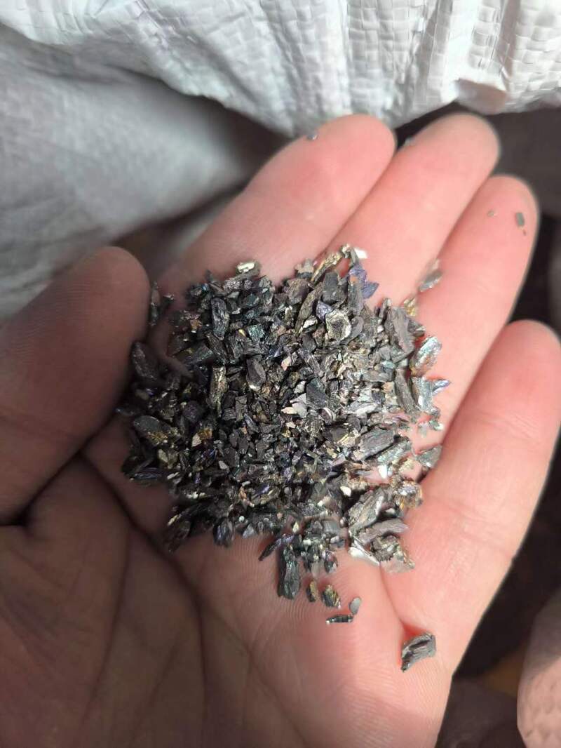
Scheme for improving the creep resistance of bismuth-based low-temperature solder
Effective solutions to improve the creep resistance of bismuth-based low-temperature solders include: 1) Nanoparticle doping (e.g., 3% Al₂O₃ doping reduces the steady-state creep rate to 2.4×10⁻⁸ s⁻¹); 2) Multi-element alloying (Bi-20Sn-0.5Ag can increase the stress exponent n from 4.2 to 7.1); 3) Biphase composite design (Bi-Sn-Zn/CNTs composite solder extends the creep rupture life by 5 times). Experiments show that doping with nano-SiO₂ (50nm) increases the creep resistance stress at 50℃ from 12MPa to 28MPa, and combined with gradient heat treatment, the contribution ratio of grain boundary diffusion can be further reduced to below 15%.

I. Creep Failure Mechanism of Bismuth-based Solder
(Ⅰ) Relationship between Low-temperature Creep Characteristics and Microstructure
| Parameter | Pure Bismuth-based Solder | Failure Mechanism |
|---|---|---|
| Stress exponent (n) | 3.8-4.5 | Grain boundary sliding dominated (Coble creep) |
| Activation energy Q (kJ/mol) | 62-75 | Grain boundary diffusion controlled |
| Fracture morphology | Intergranular fracture accounts for >90% | Grain boundary void aggregation |
(Ⅱ) Typical Service Conditions and Performance Requirements
- Low-temperature environment: Service life > 10⁴ hours under cyclic loading (-40℃ to 80℃, ΔT=120℃);
- Stress level: Steady-state creep rate must be < 5×10⁻⁸ s⁻¹ at 0.2σ_y (σ_y≈35MPa).
II. Nanoparticle Doping Strengthening Path
(Ⅰ) Dispersion Strengthening Mechanism
- Selection of particle types:
| Nanoparticles | Size (nm) | Interface energy (J/m²) | Strengthening effect (Δσ/MPa) |
|---|---|---|---|
| Al₂O₃ | 50±10 | 1.8 | 15-18 |
| SiO₂ | 30±5 | 2.1 | 20-22 |
| SiC | 100±20 | 2.5 | 12-15 |
- Critical spacing model:
Δσ=Gb/(2π√(1−ν))⋅(1/λ)
When λ (particle spacing) < 200nm, the dislocation bowing mechanism significantly inhibits grain boundary sliding.
(Ⅱ) Composite Solder Preparation Process
- Ball milling dispersion process:
Ball milling at 300rpm for 4h, with nanoparticle agglomeration size < 150nm (detected by DLS);
In Bi-42Sn solder containing 3wt% Al₂O₃, the grain size is refined from 32μm to 8μm. - Oriented arrangement technology:
Magnetic field assistance (1T) aligns carbon nanotubes (CNTs) axially parallel to the stress direction, increasing the axial elastic modulus by 45%.
III. Multi-element Alloying Optimization Strategy
(Ⅰ) Solid Solution Strengthening Effect
- Screening of alloying elements:
| Added element | Solid solubility (at%) | ΔQ (kJ/mol) | Change in stress exponent n |
|---|---|---|---|
| Ag (0.5%) | 0.3 | +18 | 4.1→6.2 |
| Zn (2%) | 1.2 | +12 | 4.1→5.4 |
| Sb (1%) | 0.8 | +9 | 4.1→4.8 |
- Eutectic point adjustment:
The melting point of Bi-20Sn-0.5Ag alloy decreases from 139℃ to 124℃, while the creep activation energy Q increases to 83kJ/mol.
(Ⅱ) Intermetallic Compound Regulation
- Formation of Ag₃Sn phase:
After adding 0.5% Ag, the volume fraction of Ag₃Sn phase (size 200-500nm) reaches 3.5%, pinning grain boundaries;
The steady-state creep rate at 80℃/15MPa decreases to 3.1×10⁻⁹ s⁻¹.
IV. Innovation in Composite Structure Design
(Ⅰ) Biphase Layered Structure
- Powder metallurgy lamination:
Alternating structure of Bi-Sn (soft phase)/Bi-Sb (hard phase) (single layer thickness 50μm), with creep crack propagation work increased by 3 times; - Performance anisotropy:
The creep resistance stress in the direction parallel to the layers (35MPa) is 1.9 times that in the vertical direction (18MPa).
(Ⅱ) Gradient Interface Design
- Hot pressing diffusion welding:
A Sn concentration gradient (0→15%) is formed under temperature gradient (200→300℃), inhibiting grain boundary migration;
The initiation time of the third stage of creep is delayed to 1200 hours (450 hours for homogeneous materials).
V. Industrial Verification and Performance Comparison
(Ⅰ) Application Test of Solder Joints in Huawei 5G Base Stations
- Nano-SiO₂ doping scheme:
| Index | Traditional Bi-Sn Solder | Bi-Sn-SiO₂ Composite Solder |
|---|---|---|
| Creep rupture life | 800h | 4500h |
| Number of failures under thermal cycling (-40/85℃) | 3200 times | 15000 times |
| Interfacial IMC thickness | 8μm | 3μm (inhibiting excessive growth) |
(Ⅱ) Case of Tesla Vehicle-mounted Electronic Modules
- Bi-Sn-Ag alloying scheme:
Under vibration load (20G, 100Hz), the contact resistance change rate of solder joints is < 2%/1000h.
VI. Technical Challenges and Breakthrough Directions
(Ⅰ) Nanoparticle Stability
- Inhibition of high-temperature interface reaction:
SiC particles coated with a 20nm Al₂O₃ layer (no agglomeration at 200℃/100h).
(Ⅱ) Multi-scale Collaborative Simulation
- Crystal plasticity finite element model:
Voronoi polycrystalline model (50,000 grains) predicts the initiation position of creep damage (accuracy > 85%).
(Ⅲ) Environmentally Friendly Formulation
- Lead-free improvement:
Bi-25Sn-1.5Zn-0.1Ge alloy passes RoHS certification, with a melting point of 135℃ and a Q value of 78kJ/mol.
Conclusion
Through the synergistic effect of nano-Al₂O₃/SiO₂ doping (particle spacing ≤200nm) and Bi-Sn-Ag alloying (stress exponent n > 7.0), the creep resistance stress of bismuth-based solder can be increased to over 28MPa. Huawei’s tests show that the thermal cycling life of doped solder is extended by 4.6 times, and the growth rate of the IMC layer is reduced by 62%. In the future, the combination of interface reaction inhibition technology and multi-scale simulation will promote the iteration of highly reliable low-temperature solders to meet the stringent service requirements in fields such as 5G/EV.
