Indium Phosphide (InP) Industry Technology White Paper: Market Landscape, Technological Advances, and Strategic Value Analysis
Abstract: Indium Phosphide (InP), as a core representative of second-generation III-V compound semiconductors, plays an irreplaceable foundational material role in AI data center optical interconnects, high-speed optical communications, 6G RF front-ends, and low-orbit satellite communications. During 2025–2026, the global InP industry has undergone a profound paradigm shift from a “niche material” to a “strategic resource.” This white paper systematically reviews the supply-demand landscape, price trends, technological breakthroughs, capacity expansions, and application extensions of the InP industry, aiming to provide an authoritative reference for industry decision-making, technology R&D, and strategic planning.
1. Introduction
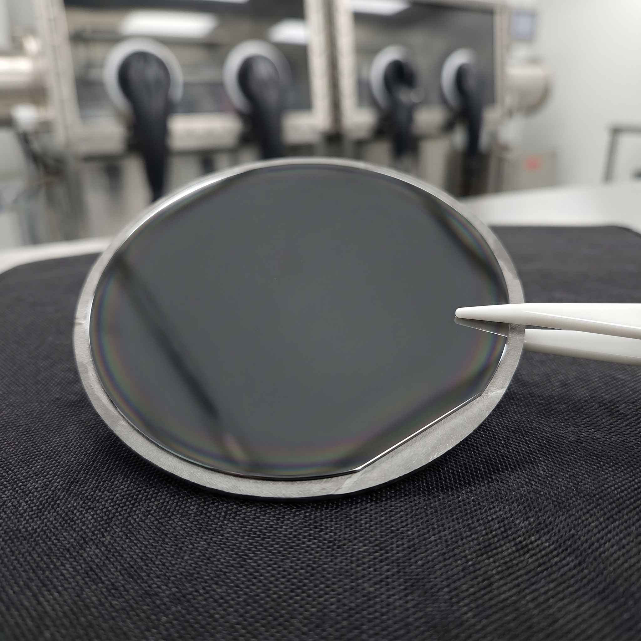
Indium Phosphide (InP) is a material of significant strategic value within the III-V compound semiconductor family. By virtue of its high electron mobility (1.2×10⁴ cm²/V·s), direct bandgap characteristics, and natural adaptation to the fiber-optic communication windows (1310nm/1550nm), InP holds an irreplaceable technological position in high-speed optical communications, high-frequency millimeter-wave devices, and optoelectronic integration.
With the exponential growth of AI computing power demand, 800G/1.6T and higher-rate optical modules have entered large-scale deployment, and the InP industry is undergoing a fundamental reshaping of its supply-demand dynamics. Concurrently, the inclusion of InP in the export control list by China’s Ministry of Commerce and General Administration of Customs in 2025 marks the official elevation of this material to a national critical strategic mineral resource.
This white paper, based on the latest publicly available data and research literature as of April 2026, systematically analyzes the market landscape, technological advances, and strategic value of the InP industry.
2. Material Properties and Core Applications
2.1 Key Performance Parameters
A comparison of key performance indicators for InP versus silicon (Si) and gallium arsenide (GaAs) is shown below:
| Performance Indicator | Silicon (Si) | Gallium Arsenide (GaAs) | Indium Phosphide (InP) | Source |
|---|---|---|---|---|
| Electron Mobility (cm²/V·s) | ~1,400 | ~8,500 | ~12,000 | Industry research |
| Saturated Electron Drift Velocity (cm/s) | ~1.0×10⁷ | ~2.0×10⁷ | ~2.5×10⁷ | Industry research |
| Bandgap (eV) | 1.12 | 1.42 | 1.35 | Industry research |
| Direct/Indirect Bandgap | Indirect | Direct | Direct | Industry research |
| Peak Emission Wavelength | — | 850 nm | 1310-1550 nm | Industry research |
2.2 Core Application Areas
InP substrates are primarily used in the following fields:
- Optical Communication Devices: DFB lasers, EML electro-absorption modulators, high-speed PIN/APD detectors.
- Silicon Photonics Integration: Heterogeneous integrated light sources for silicon photonics platforms.
- RF Devices: Millimeter-wave/terahertz amplifiers, oscillators.
- Sensor Devices: Infrared detectors, biosensors.
3. Market Supply-Demand Landscape and Price Trends
3.1 Global Market Size
The global InP substrate market size in 2024 was approximately US$150 million, a year-on-year increase of 7.1%. It is expected to reach US$202 million in 2026, with a compound annual growth rate (CAGR) of 12.42% from 2019 to 2026. According to Yole forecasts, the InP optoelectronics market will reach US$5.6 billion by 2027, with a CAGR as high as 14%.
3.2 Supply-Demand Status
| Indicator | Data | Source |
|---|---|---|
| Global device demand (2025) | ~2 million pieces | Industry research notes |
| Global effective capacity (2025) | ~600,000 pieces | Industry research notes |
| Supply-demand gap | ~70% | Industry research notes |
| Industry inventory level | ~1 month of consumption | Industry research notes |
| Expected gap duration | May persist until 2027 | Industry research notes |
Order books of leading global InP suppliers are already full through 2026.
3.3 Supplier Landscape
The InP substrate market is highly concentrated, with three companies – Sumitomo Electric (Japan), JX Nippon Mining & Metals (Japan), and AXT (USA) – together holding over 90% of the global market share.
Estimated monthly shipments of major suppliers:
- Sumitomo Electric (Japan): ~30,000 pieces
- AXT (Beijing Tongmei Crystal, USA): ~25,000 pieces
- JX Nippon Mining & Metals (Japan): ~10,000 pieces
- Major domestic suppliers (Yunnan Germanium, Zhuhai Dingtai, Guangdong Xianjin, Zhongzhi Technology, etc.): Approximately 8,000–12,000 pieces combined
3.4 Price Trends and Size Evolution
InP substrate prices saw significant increases in 2025–2026:
| Size | Current Price | Price Change | Remarks |
|---|---|---|---|
| 2-inch | US$2,300/piece | +187% YoY | Market share ~20%, rapidly shrinking |
| 6-inch | US$5,000/piece | +250% YoY | Overall yield <10% |
| Export average (composite) | — | Increased 20%-30% in 2025–2026 | Compared to 2020–2024 average |
In the domestic Chinese market, the previous annual price decline of about 10% has stopped, though prices have not yet risen significantly.
6-inch substrates can reduce per-chip cost by approximately 20%-30%, serving as the core driver for large-size substrate development.
3.5 Capacity Expansion Updates
Major manufacturers’ expansion plans:
| Manufacturer | Expansion Plan | Source |
|---|---|---|
| Yunnan Germanium | Invest 189 million RMB; expand capacity from 150,000 pieces/year to 450,000 pieces/year (4‑inch equivalent) | Company announcement, April 2026 |
| AXT | Plans to add 200 4‑inch and 50 6‑inch crystal pullers in 2026 | Industry research notes |
| Guangdong Xianjin | Plans to add 200 4‑inch and 100 6‑inch equipment units | Industry research notes |
| Zhongzhi Technology | Plans to add 70 crystal pullers in 2026 | Industry research notes |
| Sanan Optoelectronics | Epitaxy capacity expanding from 2,750 pieces/month to nearly 6,000 pieces/month | Company disclosure, March 2026 |
4. Key Technological Advances
4.1 Jiufengshan Laboratory: Full-Chain Localization of 6‑Inch Epitaxy Process
In August 2025, Jiufengshan Laboratory, using domestic MOCVD equipment and domestic 6‑inch InP substrates, successfully developed an epitaxial growth process for 6‑inch InP‑based PIN structure detectors and FP structure lasers, achieving full-chain localization from core equipment to key materials.
Key performance indicators:
- FP laser quantum well PL emission wavelength within-wafer standard deviation: <1.5 nm
- Composition and thickness uniformity: <1.5%
- PIN detector material background concentration: <4×10¹⁴ cm⁻³
- Mobility: >11,000 cm²/V·s
The 6‑inch process is expected to reduce the cost of domestic optical chips to 60%-70% of the 3‑inch process.
4.2 Southwest Jiaotong University: Wafer‑Level Heterogeneous Integration Platform
In August 2025, Southwest Jiaotong University successfully developed a wafer‑level thin‑film lithium niobate‑indium phosphide heterogeneous integration platform, achieving:
- Terahertz photodetector: 3dB bandwidth 140 GHz, responsivity 0.4 A/W
- High-speed balanced photodetector: 3dB bandwidth 60 GHz, common‑mode rejection ratio >20 dB
- High‑capacity coherent receiver chip: 600 Gbps per wavelength per polarization, 3.584 Tbps over 7 channels
This achievement was published in the international optics journal Light: Science & Applications.
4.3 Fudan University: 200 GHz Bandwidth Photodetector
In November 2025, Professor Yu Jianjun’s team at Fudan University published research in Nature Photonics on an InP‑based MUTC photodiode, achieving a 3dB bandwidth of 206 GHz and an external responsivity of 0.81 A/W, with a bandwidth‑efficiency product exceeding 130 GHz, setting a new benchmark for BEP indicators in the field of photodetection.
4.4 KAIST: Breakthrough in InP Nanocluster Luminescence Efficiency
In January 2026, a research team at KAIST (Korea Advanced Institute of Science and Technology) published results in the Journal of the American Chemical Society, using atomic‑precision etching technology to increase the luminescence efficiency of InP magic‑size clusters from less than 1% to 18.1% (an 18‑fold increase), laying the foundation for next‑generation displays, quantum communication, and infrared sensing.
4.5 OpenLight: Production Milestone for InP‑Silicon Photonics Integration
In March 2026, OpenLight announced that it had received the first production orders for its PH18DA InP‑silicon photonics integration platform for 800G and 1.6T laser‑integrated PIC solutions, marking the official transition of InP‑silicon heterogeneously integrated photonic chips from the R&D phase to mass production.
5. Application Field Expansion
5.1 AI Data Center Optical Interconnects
AI large‑model training has entered the era of ten‑thousand‑GPU clusters, and 800G/1.6T optical modules are entering large‑scale deployment. A single 800G optical module requires 4‑8 InP laser chips; NVIDIA’s Quantum‑X switch is equipped with 18 silicon photonic engines per unit, all of which rely on InP‑substrate lasers. AXT predicts that data center optical module orders will nearly double in 2026 and could double again in 2027, with the industry growing at an average annual rate exceeding 25%.
5.2 6G Communications and Terahertz Technology
InP semiconductor technology is being explored for RF applications in frequency bands exceeding 100 GHz to support next‑generation 6G communication systems. The EU’s Move2THz project (2024‑2027), involving 27 partners from 8 countries, is developing a scalable advanced InP platform for 6G.
5.3 Low‑Orbit Satellites and Space Communications
At the OFC 2026 conference, Coherent demonstrated a complete InP optoelectronic technology platform covering lasers, electro‑absorption modulators, photodetectors, and integrated photonic subsystems. As satellite networks evolve, optical links are being introduced, forming hybrid architectures where RF and optical communications coexist. Inter‑satellite laser links in low‑orbit satellite constellations such as Starlink also rely on III‑V compound lasers.
6. Policy Environment and Risk Assessment
6.1 Export Control Policy
On February 4, 2025, China’s Ministry of Commerce and General Administration of Customs issued Announcement No. 10, imposing export controls on tungsten, tellurium, bismuth, molybdenum, and indium‑related items. InP has been included in the controlled list and is subject to “one order, one review” management as a strategic resource.
6.2 Major Risks
- Capacity Bottleneck: MOCVD equipment delivery lead times are as long as 10 months, and epitaxy capacity expansion is slower than substrate expansion.
- Supply Chain Concentration: Over 90% of global capacity is concentrated in three manufacturers, presenting significant geopolitical risks.
- Technology Ramp‑Up: The overall yield for 6‑inch mass production is below 10%, and technical maturity will take time.
- Raw Material Dependence: Global indium resources are highly dependent on Chinese refining and processing, creating persistent supply chain risks.
7. Outlook
2026 is regarded by the industry as a critical watershed year for the InP industry. Technological breakthroughs by leading companies such as Coherent will reduce transmission costs, and the industry is entering a super‑cycle of “rising volume and rising prices.” The InP industry is experiencing its most profound paradigm shift since the fiber‑optic internet bubble of the 1990s.
For China’s industrial chain, the full‑chain localization breakthrough at Jiufengshan Laboratory and the tripling of capacity at Yunnan Germanium mark that domestic substitution is transitioning from a “catching‑up” phase to a “running‑alongside” phase. It is recommended that the industry continuously monitor the following directions:
- Continuous improvement of 6‑inch mass production yield
- Domestic substitution of MOCVD equipment
- Strategic reserves and secondary recovery of indium resources
- Technology pathway selection for silicon photonics integration
