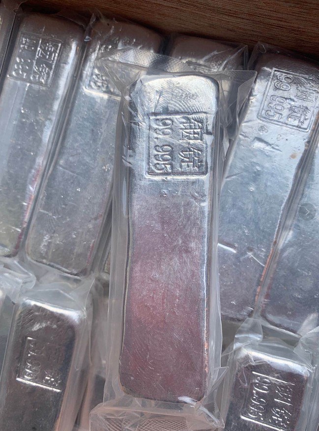
Innovative Optoelectronic Applications of Indium Compounds: Driving Next-Generation Electronics and Photonics
Abstract
Indium, a critical rare metal, has emerged as a cornerstone material for overcoming current semiconductor bottlenecks due to the unique and tunable optoelectronic properties of its compounds (e.g., indium tin oxide (ITO), indium phosphide (InP), indium selenide (InSe), and indium nitride (InN)). Recent breakthroughs in material synthesis, property modulation, and device integration have not only pushed the limits of conventional displays and photodetectors but also unlocked transformative potential in post-Moore-era integrated circuits, high-speed optical communication, and flexible electronics. This review highlights the latest innovations in indium-based materials for high-performance computing transistors, ultra-sensitive photodetectors, large-scale optoelectronic integration, and extreme-environment devices, while discussing future trends and challenges.
Introduction: The Unique Advantages of Indium
Indium is a soft, highly malleable rare metal, best known for its use in ITO transparent conductive films, the backbone of modern touchscreens. However, its potential extends far beyond. Positioned in Group IIIA of the periodic table, indium compounds exhibit high carrier mobility, tunable direct bandgaps, and exceptional optoelectronic response, making them pivotal for addressing key technological challenges:
- As silicon-based chips approach physical scaling limits, 2D indium selenide (InSe) is hailed as the “golden semiconductor” to break performance barriers.
- For high-speed optical communication, indium phosphide (InP) serves as the indispensable substrate and active material.
- In photodetection, engineered interfaces and structures in InSe, In₂O₃, and other indium compounds enable unprecedented sensitivity and speed.
The table below summarizes key indium-based materials, their properties, and cutting-edge applications:
| Material | Key Optoelectronic Properties | Innovative Applications | Recent Breakthroughs |
|---|---|---|---|
| InSe | Ultra-high mobility (>1000 cm²/V·s), low effective mass | Post-Moore transistors, flexible photodetectors | Wafer-scale 2D InSe synthesis; ferroelectric-gated detectors with record responsivity |
| InP | Direct bandgap, high saturation velocity | High-speed lasers/THz devices/quantum photonics | Domestic 6-inch InP epitaxy reduces photonic chip costs by 30–40% |
| In₂O₃ (doped) | Wide bandgap (~3.6 eV), high transparency | UV photodetectors, transparent electronics | Precise precursor control achieves responsivity of 2.53×10³ A/W |
| InTe | Narrow bandgap, pressure-induced metallization | High-pressure switches, IR detection | Light-pressure synergy lowers metallization threshold for optical switching |
| InGaN/InAlN | Continuously tunable bandgap (IR to UV) | Solid-state lighting, UV detection | Advances in epitaxial growth for high-efficiency emitters and detectors |
1. Post-Moore Electronics: The Rise of 2D Indium Semiconductors
With silicon scaling nearing its limits, InSe stands out for its near-ideal charge transport properties.
1.1 Revolutionary Material Synthesis
The 2025 breakthrough by Peking University’s Liu Kaihui team introduced a solid-liquid-solid (SLS) growth strategy to produce 2-inch single-crystalline 2D InSe wafers. By using liquid indium to regulate stoichiometry, this method solved vapor pressure disparities, enabling wafer-scale, high-purity InSe with exceptional crystallinity.
1.2 Record Device Performance
FETs fabricated from this material achieved:
- Avg. mobility: 287 cm²/V·s
- Subthreshold swing: 67 mV/dec (near Boltzmann limit)
At 10 nm channel lengths, key metrics (on/off ratio, DIBL, ballistic ratio) surpassed Intel’s 3 nm silicon nodes, even outperforming IRDS projections for 2037. This positions InSe as the top candidate to transition 2D semiconductors from labs to IC manufacturing.
2. Photodetection: From Ultra-Sensitivity to Smart Functionality
2.1 Interface Engineering for Low Noise
A team at the Institute of Physics, CAS, leveraged h-BN/InSe atomically sharp interfaces to reduce scattering, achieving:
- Mobility: 1146 cm²/V·s
- On/off ratio: 10¹⁰
With ferroelectric gating, dark current dropped to 10⁻¹⁴ A, enabling: - Responsivity: 14,250 A/W
- Detectivity: 1.63×10¹³ Jones (100× improvement)
2.2 Defect Control in In₂O₃ UV Detectors
By optimizing trimethylindium (TMIn) flow rates (50 → 5 sccm), researchers suppressed oxygen vacancies, reducing dark current by 5 orders of magnitude and achieving:
- Light/dark current ratio: 2589
- Responsivity: 2.53×10³ A/W (record high)
2.3 Extreme-Environment Applications
Tianjin University discovered that green light excitation lowers InTe’s metallization pressure threshold from 5.0 GPa to 4.4 GPa, enabling light-controlled pressure sensors for deep-sea/geological exploration.
3. Optoelectronic Integration: Scaling Up with Domestic Innovation
InP is the backbone of optical communication lasers and detectors.
3.1 6-Inch InP Epitaxy Breakthrough
In 2025, Jiufengshan Lab achieved full domestic production of 6-inch InP-based lasers/detectors via homegrown MOCVD systems and substrates, slashing photonic chip costs by 30–40% versus 3-inch platforms. This milestone strengthens China’s supply chain in high-speed modules, LiDAR, and THz communication.
4. Conclusion and Outlook
Indium-based materials are revolutionizing electronics and photonics through 2D engineering, defect control, and large-scale epitaxy. Key advances include:
- InSe transistors extending Moore’s Law.
- InSe/In₂O₃ detectors with near-ultimate sensitivity.
- 6-inch InP wafers enabling cost-effective photonics.
Challenges remain:
- Scalable InSe wafer production and integration.
- Indium scarcity necessitates recycling/alternatives.
- Reliability and standardization for industrial adoption.
Future innovations will focus on heterogeneous integration with silicon CMOS and AI-driven optoelectronic computing, reshaping the technological landscape.
