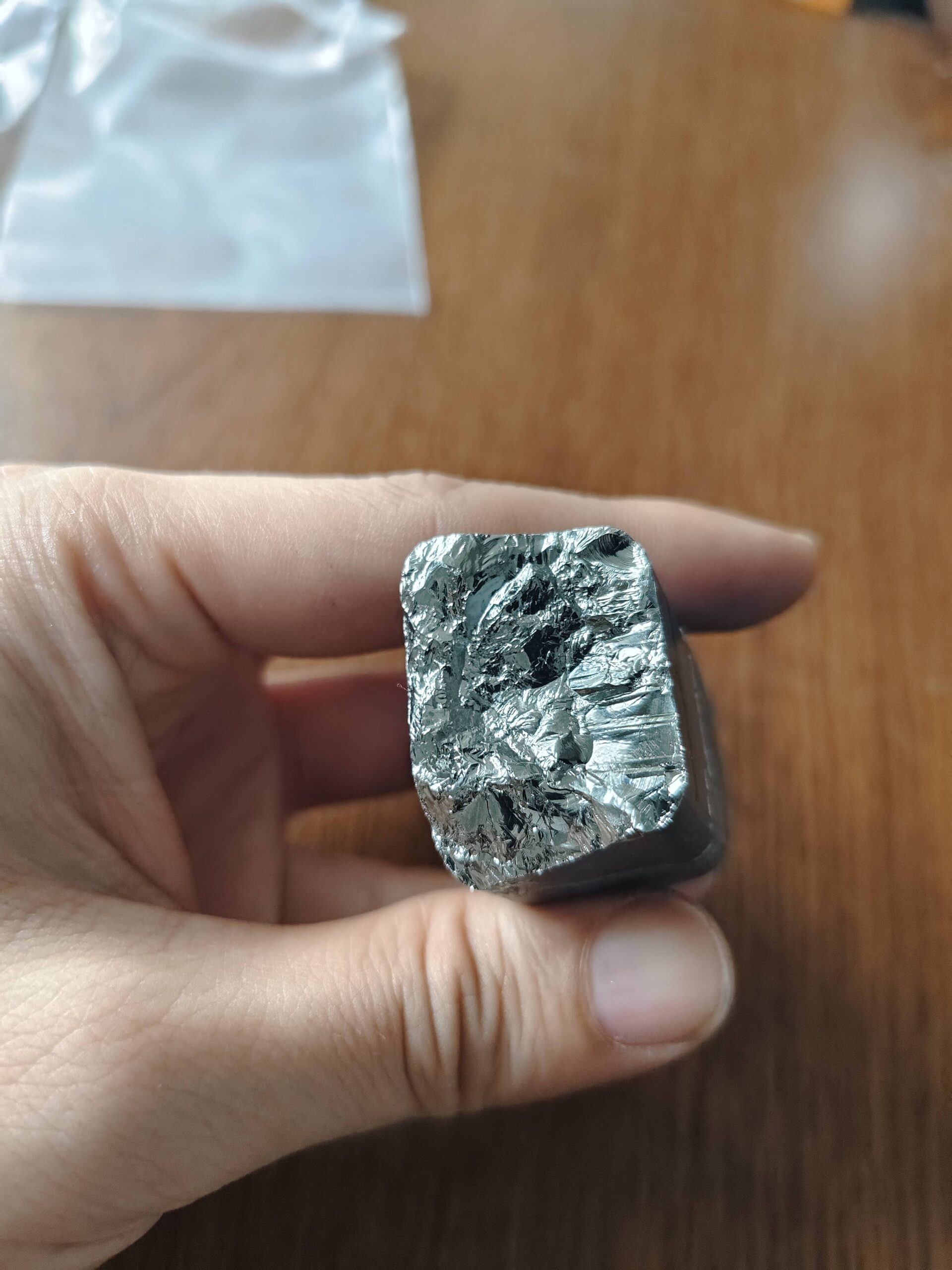
Key Process Parameters Control and Defect Avoidance in Germanium Single Crystal Growth
Abstract
In the growth of germanium single crystals, critical process parameters include growth temperature, growth pressure, growth rate, and the relative positioning between seed crystal and melt. Optimizing these parameters—such as employing vertical growth methods and precise temperature control—effectively reduces dislocations and defects, thereby enhancing the electrical performance of the crystals. Annealing treatments further decrease defect density and improve carrier mobility. Additionally, doping techniques that introduce specific impurity elements (e.g., boron or phosphorus) enable fine-tuning of the crystal’s conductivity and semiconductor properties, facilitating performance optimization.
1.Key Process Parameters in Germanium Single Crystal Growth
The quality of germanium single crystals strongly depends on the precise control of several key process parameters:
1.1 Growth Temperature
The growth temperature directly affects melt stability and crystal nucleation. Excessively high temperatures may cause volatilization of melt components or impurity incorporation, while too low temperatures can lead to uneven crystal growth. Studies indicate that maintaining the temperature within ±5°C of germanium’s melting point significantly reduces dislocation defects induced by thermal stress.
1.2 Growth Pressure
Growth pressure must be coordinated with temperature to sustain chemical equilibrium in the melt. Low-pressure environments promote component volatilization, whereas high pressure can inhibit impurity diffusion. Typically, an inert gas atmosphere (e.g., argon) is used to maintain pressure between 10 and 100 Torr, balancing melt stability with defect suppression.
1.3 Growth Rate
Excessively fast growth rates introduce supercooling, causing lattice distortion; overly slow rates reduce production efficiency. Experimental results suggest that a growth rate of 0.5–2 mm/min optimizes crystal quality and growth throughput.
1.4 Relative Positioning of Seed Crystal and Melt
Vertical growth methods minimize melt convection disturbances to the crystal, lowering dislocation density. The orientation of the seed crystal (e.g., <111> or <100>) also influences defect distribution and should be selected based on application requirements.
2.Methods to Suppress Crystal Defects
2.1 Annealing Treatment
Annealing is crucial for relieving internal stresses and reducing defects. Slowly heating to 600–800°C followed by holding allows dislocation glide and rearrangement, and impurity atoms diffuse to grain boundaries. Optimized annealing can reduce Schottky barrier height by 30% and increase carrier mobility by 20%.
2.2 Doping Techniques
Doping enables targeted control of electrical properties:
·Boron doping enhances p-type conductivity, suitable for high-frequency devices;
·Phosphorus doping strengthens n-type characteristics, applied in photodetectors.
Dopant concentrations must be precisely controlled (typically 10^15–10^18 atoms/cm³) to avoid carrier scattering or lattice distortion.
2.3 Environmental Control
·High-purity raw materials reduce native impurities such as oxygen and carbon;
·Sealed growth systems prevent external contamination and ensure stable stoichiometry.
3.Process Optimization and Performance Enhancement
By comprehensive regulation of the above parameters, electronic-grade germanium single crystals achieve:
·Room-temperature resistivity as low as 10^-9 Ω·cm;
·Carrier mobility reaching 1000 cm²/V·s;
·Defect density reduced below 10^3 cm^-2.
4.Future Development Directions
Further research should focus on:
·Developing multiparameter coupled models that mathematically describe temperature-pressure-rate interactions;
·Innovating doping techniques such as co-doping or gradient doping to broaden application possibilities;
·Implementing in-situ monitoring technologies for real-time growth feedback and dynamic control.
Optimizing germanium single crystal growth processes not only improves material properties but also lays the foundation for miniaturized, high-performance semiconductor devices. With ongoing technological innovation, germanium-based materials are expected to play an increasingly significant role in optoelectronic integration and quantum computing.
