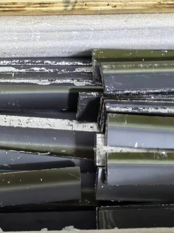
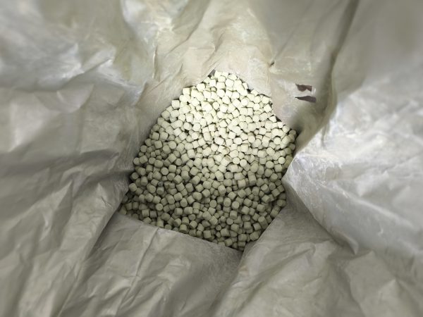
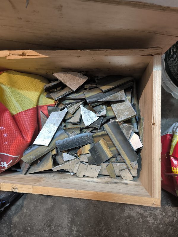
ITO (Indium Tin Oxide) target material is a high-density ceramic bulk material, fabricated by sintering ITO target powder (indium oxide In₂O₃ doped with tin oxide SnO₂). It is a core consumable for preparing ITO transparent conductive films via magnetron sputtering. Its performance directly determines the conductivity, light transmittance, and uniformity of the films, making it widely used in electronic information fields such as displays, photovoltaics, and touch panels. Here is a detailed introduction:
- Chemical Composition: Based on indium oxide (In₂O₃) as the matrix, doped with 5%-10% (molar ratio) tin oxide (SnO₂). Tin ions (Sn⁴⁺) replace some indium ions (In³⁺) to form free electrons, endowing the material with conductivity; the cubic bixbyite structure of indium oxide ensures high visible light transmittance.
- Key Physical Properties:
- Density: Must reach over 95% of the theoretical density (ideally 98%-99%) to avoid “particulate” defects caused by internal pores during sputtering, which would affect film quality.
- Purity: Industrial-grade targets are typically 99.99% (4N), while high-end applications (e.g., semiconductors) require 99.999% (5N). Impurities such as alkali metals and heavy metals are strictly controlled (content <1ppm) to prevent increased film resistivity.
- Microstructure: Uniform grains (5-20μm in size) and no segregation ensure consistency in sputtering rate and film performance.
- Mechanical Properties: Flexural strength >150MPa and hardness >500HV to meet mechanical stability during sputtering (preventing target cracking).
The preparation of ITO targets involves converting ITO target powder into dense ceramics through high-temperature sintering, with core steps including:
-
Powder Pretreatment:
The target powder must have controlled particle size (1-5μm), specific surface area (>10m²/g), and particle size distribution (D50 <3μm). Uniform mixing is achieved via ball milling or air jet milling to avoid compositional segregation during subsequent sintering.
-
Forming:
- Small targets: Dry pressing (pressure 100-300MPa);
- Large/irregular targets (e.g., 1.5m-grade targets for G10.5 displays): Cold isostatic pressing (CIP, pressure 200-400MPa) to ensure uniform green body density (>65% of theoretical density).
-
Sintering:
- Atmosphere: Sintered in oxygen or air (to inhibit In₂O₃ decomposition);
- Temperature and Time: Held at 1400-1600℃ for 10-20 hours. Particle bonding and pore elimination occur via diffusion sintering;
- Innovative Processes: Microwave sintering (shortening time to 2-4 hours) and spark plasma sintering (SPS, low-temperature rapid densification) improve efficiency but with higher costs.
-
Post-Processing:
After cutting, grinding (surface roughness Ra <0.5μm), and bonding (welding to copper/molybdenum backing plates for enhanced heat dissipation), the final targets are ready for direct installation in sputtering equipment.
ITO targets are categorized by shape and application:
- Planar Targets: Simple structure, suitable for small-to-medium area film deposition (e.g., mobile phone screens, small-sized photovoltaic cells), but with low utilization (only 30%-40%).
- Rotary Targets: Tubular in shape, enabling uniform sputtering via rotation, with utilization increased to 60%-80%. They are mainstream for large-area, high-production scenarios (e.g., 8K TV panels, G8.5+ display production lines).
Core Applications:
- Display Sector: Pixel electrodes in LCD/OLED panels and conductive layers in touch screens, requiring film transmittance >90% and resistivity <10⁻⁴Ω·cm.
- Photovoltaic Industry: Front/back transparent electrodes in heterojunction (HJT) solar cells, balancing high transmittance (especially in the near-infrared region) and low contact resistance.
- Functional Coatings: Smart glass (electrochromic), electromagnetic shielding films, and sensor electrodes, relying on target stability and film uniformity.
- Sputtering Stability: Target composition uniformity error must be <0.5%; otherwise, film resistivity fluctuations (>5%) may occur.
- Impurity Control: Alkali metal (Na, K) content <0.1ppm to prevent ion migration in films at high temperatures; carbon and hydrogen impurities can cause “black ash” defects during sputtering.
- Dimensional Accuracy: Straightness error of large rotary targets <0.1mm/m to ensure uniform gaps with sputtering equipment (affecting film thickness deviation).
- Market Size: The global ITO target market was ~$4.5 billion in 2023, projected to reach $6.8 billion by 2028, with China accounting for over 50% (mainly for display panels).
- Key Enterprises:
- Japan: JX Nippon Mining & Metals (high-end targets, semiconductor-grade), Sumitomo Metal;
- China: Xian Dao Rare Materials (global leading rotary target production capacity), Hengtong Optic-Electric (G10.5-grade large-size targets);
- South Korea: Samsung SDI (supporting local display industry chains).
- Critical Challenges:
- Indium Resource Constraints: Global indium reserves are only ~50,000 tons, with indium accounting for >70% of target costs. Price fluctuations ($300-400/kg in 2023-2025) affect industry stability.
- Competition from Alternatives: AZO (aluminum-doped zinc oxide), silver nanowires, and graphene aim to replace ITO but still lag in comprehensive performance (transmittance + conductivity + stability).
- Large-Scale and Thin-Substrate Trends: G11 display panels (3370×2940mm) require targets over 3m in length, and sintering thin targets (thickness <5mm) is significantly more challenging.
- High Density and Low Defects: Sintering with nano-target powder (particle size <100nm) to achieve target density >99%, reducing film particulate defects.
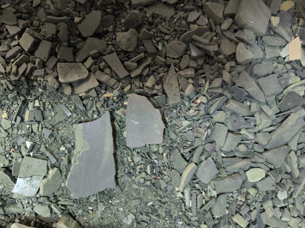
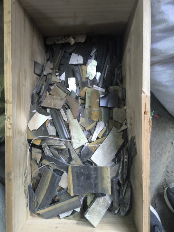
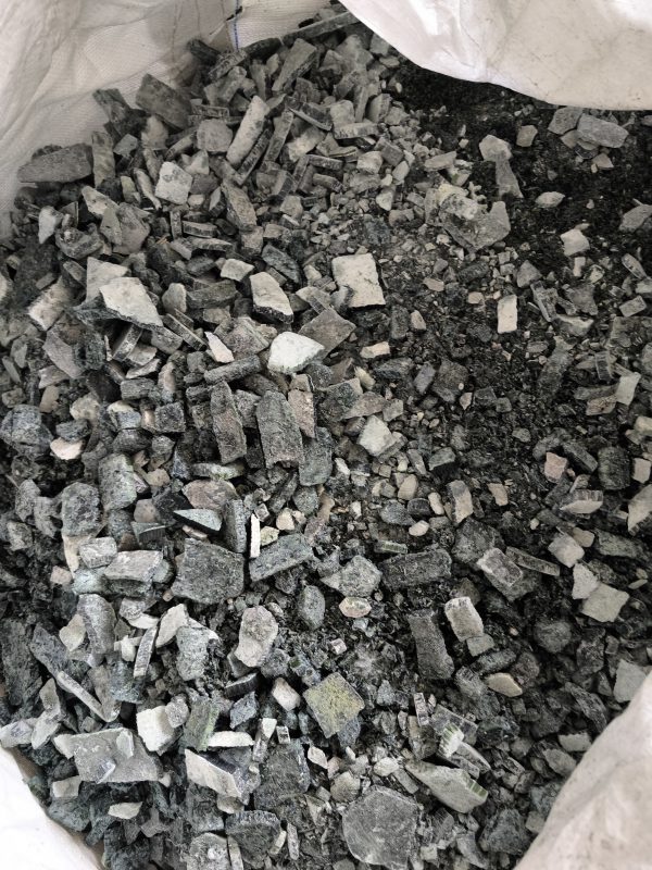
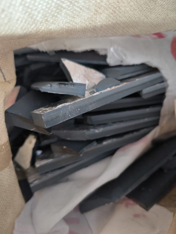
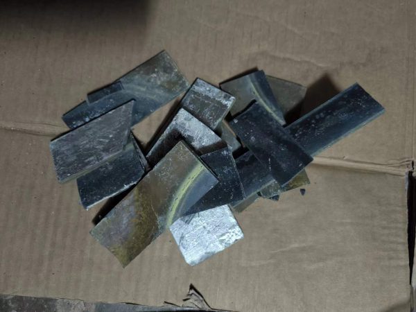
- Recycling and Circular Utilization: Over 90% of indium can be recovered from retired targets via acid dissolution and purification. Global indium recycling accounted for 35% in 2025, projected to reach 50% by 2030.
- Composite Targets: Doping with gallium (Ga), zinc (Zn), etc., to optimize ITO film weather resistance (e.g., anti-high-temperature yellowing) for flexible display needs.
ITO target material is a core link connecting upstream indium resources and downstream electronic devices, with its performance directly determining the quality of end products. Despite resource constraints and substitution pressures, its irreplaceability in high-resolution displays, high-efficiency photovoltaics, and other fields remains unshakable in the short term. Future innovations in efficient indium utilization, target performance upgrading, and green manufacturing will drive the continuous development of the ITO target industry.





Reviews
There are no reviews yet.